ESR (Electron Spin Resonance) Spectroscopy Laboratory Takahide Umeda’s laboratory | University of Tsukuba, Institute of Applied Physics
ESR spectroscopy for semiconductor materials
ESR (Electron Spin Resonance) is one of the most useful spectroscopy for identifying the origins of energy-gap levels in semiconductor materials. ESR spectrum is very sensitive to the eigen wave functions of such energy levels, which makes it possible to determine the microscopic origins of the levels. Usually, the energy-gap levels originate from lattice defects and impurities in semiconductor materials. Thus, ESR is a highly sensitive probe for defects and impurities in semiconductors. ESR can also detect carriers in the conduction and valence bands of semiconductors, giving us another interesting information. Using ESR and related techniques, we investigate a lot of defects and impurities in semiconductor materials such as silicon (Si) and silicon carbide (SiC). Kindly find many examples in our publication list.
 |
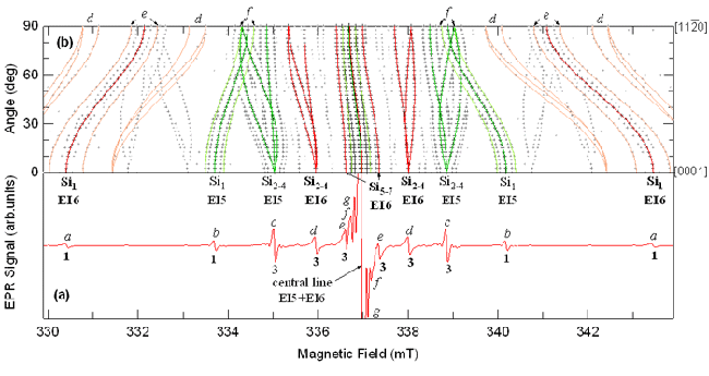
| Fig. 1. ESR spectrum of carbon vacancy in SiC |
| This example shows an ESR spectrum of the EI5/6 centers (carbon vacancies) in 4H-SiC. This spectrum involves 29Si hyperfine structures due to four silicon neighbors of a carbon vacancy. This spectrum enables a final identification of carbon vacancies in SiC. See details in T. Umeda et al., Phys. Rev. B 69, 121201(R) (2004). |
 |
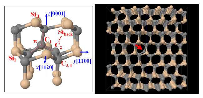
| Fig. 2. Carbon interstitial defects in SiC |
| Silicon Carbide (SiC) is one of the best semiconductor materials for power electronics. We have identified a lot of fundamental defects in SiC. This example shows a “carbon interstitial defect” in 4H-SiC, which is one of the key defects for SiC crystals and devices. See details in T. Umeda et al., Phys. Rev. B 79, 115211 (2009). |
 |
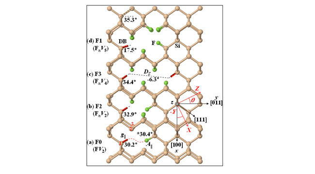
| Fig. 3. Fluorine in Silicon |
| Fluorine has a unique chemical character and is often introduced into Si micro-devices via ion-implantation processes. This example shows various forms of fluorine atoms in silicon, which have been revealed by our ESR study. See details in T. Umeda et al., Appl. Phys. Lett. 97, 041911 (2010). |
[Page top]