Defect dat@base
Our lablatory presents two database sites for ESR and defects in semiconductor materials. These databases are opened on Web sites and now get worldwide access with an average of 1.98 millions pages/month (a period from Apr. 2006 to Jan. 2010).
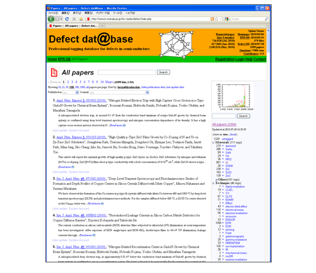 |
| Fig. 7. “Defect dat@base” |
| http://www.kc.tsukuba.ac.jp/div-media/defect/ This Web site features important papers that described defects in semiconductor materials. These papers are classified by the “social tagging” system in cooperation with specialists over the world. See details in T. Umeda and S. Hagiwara et al., JOHO KANRI (J. Information Processing and Management) 51, 653-662 (2008). |
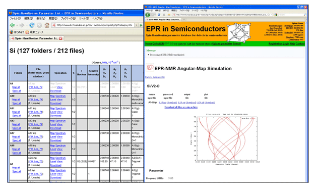 |
| fig. 8. “EPR in Semiconductors” |
| http://www.kc.tsukuba.ac.jp/div-media/epr/ This Web site offers a database of ESR (EPR) parameters for various defect centers in semiconductor materials. Furthermore, using the stored parameters, we can simulate angular-pattern, ESR spectrum, and spin eigenlevels via the EPR-NMR(c) simulator that has been developed by the famous ESR group of Prof. J. A. Weil (University of Saskatchewan, Canada). New ESR (EPR) parameters can be uploaded from ESR specialists. See details in T. Umeda, S. Hagiwara et al., Physica B 376-377, 249 (2006). |
[Page top]